[ad_1]
One in every of us (Levi) works with semiconductors and the opposite (Aeppli) with X-rays. So, after pondering this downside, we thought-about utilizing X-rays to nondestructively picture chips. You’d have to transcend the decision utilized in medical X-ray scanners. However it was clear to us that the wanted decision was attainable. At that second, what we’ve been calling the “chip scan” mission was born.
 Our first method, ptychographic X-ray computed tomography, was examined first on a portion of a 22-nanometer Intel processor developing an in depth 3D picture of the chip’s interconnects.SLS-USC Chip-Scan workforce
A number of years later, we’ve made it attainable to map the complete interconnect construction of even probably the most superior and complicated processors with out destroying them. Proper now, that course of takes greater than a day, however enhancements over the following few years ought to allow the mapping of total chips inside hours.
This system—known as ptychographic X-ray laminography—requires entry to a number of the world’s strongest X-ray mild sources. However most of those services are, conveniently, positioned near the place a lot of the superior chip design occurs. In order entry to this system expands, no flaw, failure, or fiendish trick will be capable of disguise.
After deciding to pursue this method, our first order of enterprise was to ascertain what state-of-the-art X-ray strategies may do. That was completed on the Paul Scherrer Institute (PSI) in Switzerland, the place one in every of us (Aeppli) works. PSI is residence to the Swiss Mild Supply (SLS) synchrotron, one of many 15 brightest sources of coherent X-rays constructed up to now.
Coherent X-rays differ from what’s utilized in a medical or dental workplace in the identical method that the extremely collimated beam of sunshine from a laser pointer differs from mild emitted in all instructions from an incandescent bulb. The SLS and related services generate extremely coherent beams of X-ray photons by first accelerating electrons nearly to the pace of sunshine. Then, magnetic fields deflect these electrons, inducing the manufacturing of the specified X-rays.
To see what we may do with the SLS, our multidisciplinary workforce purchased an Intel Pentium G3260 processor from a neighborhood retailer for about US $50 and eliminated the packaging to show the silicon. (This CPU was manufactured utilizing 22-nanometer CMOS FinFET know-how).
A fly-though of the highest layers of an Intel 22-nanometer processor reconstructed from X-ray scans.SLS-USC Chip-Scan Staff
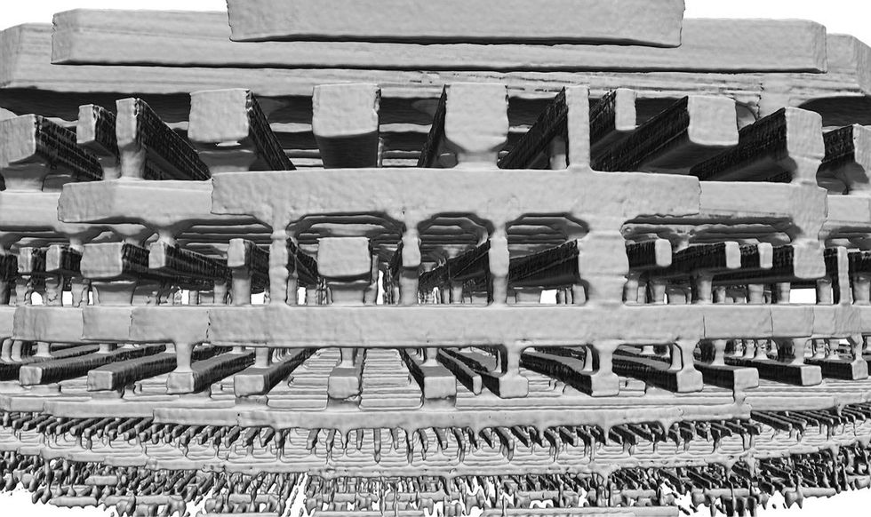
Like all such chips, the G3260’s transistors are made from silicon, but it surely’s the association of metallic interconnects that hyperlink them as much as kind circuits. In a contemporary processor, interconnects are constructed in additional than 15 layers, which from above appear like a map of a metropolis’s road grid. The decrease layers, nearer to the silicon, have extremely effective options, spaced simply nanometers aside in in the present day’s most superior chips. As you ascend the interconnect layers, the options grow to be sparser and greater, till you attain the highest, the place electrical contact pads join the chip to its package deal.
We started our examination by slicing out a 10-micrometer-wide cylinder from the G3260. We needed to take this harmful step as a result of it tremendously simplified issues. Ten micrometers is lower than half the penetration depth of the SLS’s photons, so with one thing this small we’d be capable of detect sufficient photons passing by way of the pillar to find out what was inside.
We positioned the pattern on a mechanical stage to rotate it about its cylindrical axis after which fired a coherent beam of X-rays by way of the aspect. Because the pattern rotated, we illuminated it with a sample of overlapping 2-µm-wide spots.
At every illuminated spot, the coherent X-rays diffracted as they handed by way of the chip’s tortuous tower of copper interconnects, projecting a sample onto a detector, which was saved for subsequent processing. The recorded projections contained sufficient details about the fabric by way of which the X-rays traveled to find out the construction in three dimensions. This method is named ptychographic X-ray computed tomography (PXCT). Ptychography is the computational course of of manufacturing a picture of one thing from the interference sample of sunshine by way of it.
The underlying precept behind PXCT is comparatively easy, resembling the diffraction of sunshine by way of slits. You would possibly recall out of your introductory physics class that in the event you shine a coherent beam of sunshine by way of a slit onto a distant aircraft, the experiment produces what’s known as a Fraunhofer diffraction sample. This can be a sample of sunshine and darkish bands, or fringes, spaced proportionally to the ratio of the sunshine’s wavelength divided by the width of the slit.
If, as a substitute of shining mild by way of a slit, you shine it on a pair of carefully spaced objects, ones so small that they’re successfully factors, you’re going to get a special sample. It doesn’t matter the place within the beam the objects are. So long as they keep the identical distance from one another, you possibly can transfer them round and also you’d get the identical sample.
By themselves, neither of those phenomena will allow you to reconstruct the tangle of interconnects in a microchip. However in the event you mix them, you’ll begin to see the way it may work. Put the pair of objects inside the slit. The ensuing interference sample is derived from the diffraction as a consequence of a mixture of slit and object, revealing details about the width of the slit, the gap between the objects, and the relative place of the objects and the slit. For those who transfer the 2 factors barely, the interference sample shifts. And it’s that shift that means that you can calculate precisely the place the objects are inside the slit.
Any actual pattern will be handled as a set of pointlike objects, which give rise to complicated X-ray scattering patterns. Such patterns can be utilized to deduce how these pointlike objects are organized in two dimensions. And the precept can be utilized to map issues out in three dimensions by rotating the pattern inside the beam, a course of known as tomographic reconstruction.
You want to ensure you’re set as much as gather sufficient knowledge to map the construction on the required decision. Decision is set by the X-ray wavelength, the dimensions of the detector, and some different parameters. For our preliminary measurements with the SLS, which used 0.21-nm-wavelength X-rays, the detector needed to be positioned about 7 meters from the pattern to succeed in our goal decision of 13 nm.
In March 2017, we demonstrated the usage of PXCT for nondestructive imaging of built-in circuits by publishing some very fairly 3D photos of copper interconnects within the Intel Pentium G3260 processor. These photos reveal the three-dimensional character and complexity {of electrical} interconnects on this CMOS built-in circuit. However additionally they captured attention-grabbing particulars such because the imperfections within the metallic connections between the layers and the roughness between the copper and the silica dielectric round it.
From this proof-of-principle demonstration alone, it was clear that the method had potential in failure evaluation, design validation, and high quality management. So we used PXCT to probe equally sized cylinders minimize from chips constructed with different corporations’ applied sciences. The small print within the ensuing 3D reconstructions had been like fingerprints that had been distinctive to the ICs and likewise revealed a lot concerning the manufacturing processes used to manufacture the chips.
We had been inspired by our early success. However we knew we may do higher, by constructing a brand new sort of X-ray microscope and arising with more practical methods to enhance picture reconstruction utilizing chip design and manufacturing data. We known as the brand new method PyXL, shorthand for ptychographic X-ray laminography.
The very first thing to cope with was learn how to scan a complete 10-millimeter-wide chip after we had an X-ray penetration depth of solely round 30 µm. We solved this downside by first tilting the chip at an angle relative to the beam. Subsequent, we rotated the pattern concerning the axis perpendicular to the aircraft of the chip. On the identical time we additionally moved it sideways, raster style. This allowed us to scan all components of the chip with the beam.
At every second on this course of, the X-rays passing by way of the chip are scattered by the supplies contained in the IC, making a diffraction sample. As with PXCT, diffraction patterns from overlapping illumination spots include redundant details about what the X-rays have handed by way of. Imaging algorithms then infer a construction that’s the most in step with all measured diffraction patterns. From these we will reconstruct the inside of the entire chip in 3D.
Evidently, there may be loads to fret about when growing a brand new sort of microscope. It will need to have a steady mechanical design, together with exact movement phases and place measurement. And it should document intimately how the beam illuminates every spot on the chip and the following diffraction patterns. Discovering sensible options to those and different points required the efforts of a workforce of 14 engineers and physicists. The geometry of PyXL additionally required growing new algorithms to interpret the information collected. It was onerous work, however by late 2018 we had efficiently probed 16-nm ICs, publishing the ends in October 2019.
In the present day’s cutting-edge processors can have interconnects as little as 30 nm aside, and our method can, no less than in precept, produce photos of buildings smaller than 2 nm.
In these experiments, we had been ready to make use of PyXL to peel away every layer of interconnects just about to disclose the circuits they kind. As an early check, we inserted a small flaw into the design file for the interconnect layer closest to the silicon. Once we in contrast this model of the layer with the PyXL reconstruction of the chip, the flaw was instantly apparent.
In precept, a few days of labor is all we’d want to make use of PyXL to acquire significant details about the integrity of an IC manufactured in even probably the most superior services. In the present day’s cutting-edge processors can have interconnects simply tens of nanometers aside, and our method can, no less than in precept, produce photos of buildings smaller than 2 nm.
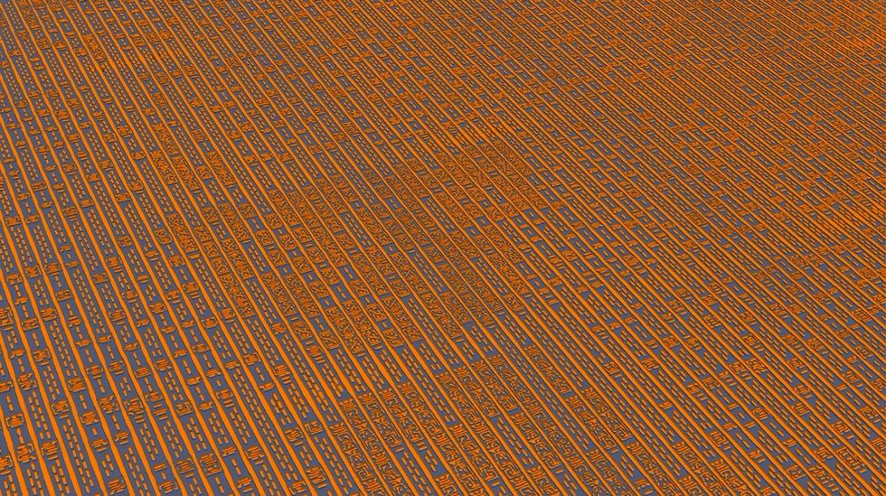
The brand new model of our X-ray method, known as ptychographic X-ray laminography, can uncover the interconnect construction of total chips with out damaging them, even all the way down to the smallest buildings [top]. Utilizing that method, we may simply uncover a (deliberate) discrepancy between the design file and what was manufactured [bottom].
However elevated decision does take longer. Though the {hardware} we’ve constructed has the capability to utterly scan an space as much as 1.2 by 1.2 centimeters on the highest decision, doing so can be impractical. Zooming in on an space of curiosity can be a greater use of time. In our preliminary experiments, a low-resolution (500-nm) scan over a sq. portion of a chip that was 0.3 mm on a aspect took 30 hours to amass. A high-resolution (19-nm) scan of a a lot smaller portion of the chip, simply 40 μm huge, took 60 hours.
The imaging price is essentially restricted by the X-ray flux out there to us at SLS. However different services boast increased X-ray fluxes, and strategies are within the works to spice up X-ray supply “brilliance”—a mixture of the variety of photons produced, the beam’s space, and the way shortly it spreads. For instance, the MAX IV Laboratory in Lund, Sweden, pioneered a method to enhance its brilliance by two orders of magnitude. An extra one or two orders of magnitude will be obtained via new X-ray optics. Combining these enhancements ought to in the future enhance whole flux by an element of 10,000.
With this increased flux, we must always be capable of obtain a decision of two nm in much less time than it now takes to acquire 19-nm decision. Our system may additionally survey a one-square-centimeter built-in circuit—concerning the measurement of an Apple M1 processor—at 250-nm decision in fewer than 30 hours.
And there are different methods of boosting imaging pace and backbone, reminiscent of higher stabilizing the probe beam and enhancing our algorithms to account for the design guidelines of ICs and the deformation that may outcome from an excessive amount of X-ray publicity.
Though we will already inform so much about an IC from simply the format of its interconnects, with additional enhancements we must always be capable of uncover the whole lot about it, together with the supplies it’s made from. For the 16-nm-technology node, that features copper, aluminum, tungsten, and compounds known as silicides. We would even be capable of make native measurements of pressure within the silicon lattice, which arises from the multilayer manufacturing processes wanted to make cutting-edge gadgets.
Figuring out supplies may grow to be notably necessary, now that copper-interconnect know-how is approaching its limits. In modern CMOS circuits, copper interconnects are vulnerable to electromigration, the place present can kick copper atoms out of alignment and trigger voids within the construction. To counter this, the interconnects are sheathed in a barrier materials. However these sheaths will be so thick that they go away little room for the copper, making the interconnects too resistive. So various supplies, reminiscent of cobalt and ruthenium, are being explored. As a result of the interconnects in query are so effective, we’ll want to succeed in sub-10-nm decision to differentiate them.
There’s purpose to suppose we’ll get there. Making use of PXCT and PyXL to the “connectome” of each {hardware} and wetware (brains) is among the key arguments researchers world wide have made to help the development of recent and upgraded X-ray sources. Within the meantime, work continues in our laboratories in California and Switzerland to develop higher {hardware} and software program. So sometime quickly, in the event you’re suspicious of your new CPU or interested by a competitor’s, you could possibly make a fly-through tour by way of its internal workings to ensure the whole lot is admittedly in its correct place.
The SLS-USC Chip-Scan Staff contains Mirko Holler, Michal Odstrcil, Manuel Guizar-Sicairos, Maxime Lebugle, Elisabeth Müller, Simone Finizio, Gemma Tinti, Christian David, Joshua Zusman, Walter Unglaub, Oliver Bunk, Jörg Raabe, A. F. J. Levi, and Gabriel Aeppli.
This text seems within the Could 2022 print concern as “The Bare Chip.”
Source link